Ink Laydown and Opacity: pad printing vs silk screening Compared
Views: 3 Author: Allen Xiao Publish Time: 2026-03-15


Branding integrity in the hardware sector is anchored by the durability and precision of surface markings. When an engineer designs a medical diagnostic device or an industrial control panel, the legibility of safety warnings, corporate logos, and interface labels is not a cosmetic luxury; it is a functional requirement for long-term field survival. In the uncompromising domain of Injection molding surface finishes, choosing the incorrect method to apply graphics can lead to catastrophic "Logo Erosion" under the assault of cleaning chemicals or repetitive human contact. Navigating the standoff of pad printing vs silk screening requires a forensic understanding of ink laydown physics and geometric conformity. If your part possesses complex 3D curves or ultra-fine details, one process acts as a precision scalpel, while the other functions as a high-saturation heavy lifter. Jucheng Precision operates as a high-fidelity secondary operations hub, navigating these mechanical discrepancies to ensure your Injection molding materials are armored with immutable visual data.

Surface topography dictates the success of ink transfer. Amateurs often attempt to silk-screen logos onto curved smartphone accessories, resulting in smeared edges and inconsistent coverage. Professional manufacturing sovereignty requires matching the printing mechanism to the part’s "Line of Draw." Jucheng Precision eliminates these "Graphic Disasters" by offering both elite pad printing and high-tension silk screening under a single roof. We understand that the molecular bond between the ink and the polymer substrate must survive the ASTM D3359 "Tape Test" while maintaining the color fidelity of your brand. This guide deconstructs the mechanical divide between the silicone pad and the mesh screen, the physics of ink thickness, and the strategic selection matrix needed to secure retail-ready aesthetics for your most ambitious hardware projects.
content:
Pad Printing Dynamics: Conforming to 3D Contours
Silk Screening Sovereignty: Opacity on Flat Planes
Ink Physics: Layer Thickness and Abrasion Resistance
The Selection Matrix: Mapping Geometry to Printing Logic
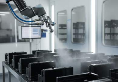
JUCHENG Protocol: Integrated Secondary Operations and QC
Pad Printing Dynamics: Conforming to 3D Contours

Mechanical versatility represents the core advantage of pad printing (Tampo Printing). This process functions as an "Offset" transfer method, utilizing a soft, highly deformable silicone pad to pick up ink from an etched steel plate (cliché) and deposit it onto the plastic component. The beauty of pad printing vs silk screening in this context is the pad's ability to wrap around spherical surfaces, reach into deep recesses, and print across textured ridges without distorting the graphic. At Jucheng Precision, we calibrate the "Shore Durometer" of the silicone pad to match your part’s specific radius. A soft pad allows for extreme 3D wrapping, while a harder pad ensures the crispness of microscopic text on a curved medical stylus. Because the ink is picked up as a thin film from the etched cliché, the resolution is spectacular—capable of resolving text as small as 4pt. This makes it the mandatory choice for consumer electronics with complex ergonomic shapes and medical devices requiring precision serial numbers on non-flat housings.
Silk Screening Sovereignty: Opacity on Flat Planes

Opacity and saturation dictate the visual dominance of large-format graphics. Silk screening (Screen Printing) operates by forcing thick, viscous ink through a fine mesh stencil using a high-pressure rubber squeegee. In the standoff of pad printing vs silk screening, the mesh-based approach is the undisputed king of "Ink Volume." Because the ink is pushed directly through the open areas of the screen, we can achieve an ink laydown thickness of up to 30 microns—nearly four times thicker than pad printing. This high volume creates vibrant, punchy colors that are completely opaque, even when printing a white logo onto a pitch-black resin. Jucheng Precision utilizes silk screening for flat-panel interfaces, industrial equipment enclosures, and large-format lids where the graphic must withstand years of solar exposure without fading. The limitation, however, is purely geometric: the screen must maintain a parallel distance to the part surface, effectively restricting this process to flat planes or very gentle single-axis curves.
Ink Physics: Layer Thickness and Abrasion Resistance

Chemical and mechanical durability are directly tied to the "Ink Profile" left on the part. While the thicker layer of silk screening provides superior UV stability and color depth, the ultra-thin layer of pad printing offers a strategic advantage for assembly. A pad-printed logo adds negligible thickness to a part (approx. 5-8 microns), meaning it won't interfere with the fit of a tight-tolerance snap-fit or the travel of a sliding switch. To assist in process selection, Jucheng Precision provides the following technical comparison:
| Feature | Pad Printing | Silk Screening |
|---|---|---|
| Geometric Capability | High 3D Curves / Irregular | Flat Surfaces Only |
| Ink Thickness | Thin (4 - 10 µm) | Thick (20 - 35 µm) |
| Detail Resolution | Extreme (Micro-text) | Moderate (Bold Icons) |
| Opacity/Brightness | Moderate (Double-strike needed) | Superior |
The Selection Matrix: Mapping Geometry to Printing Logic

Strategic routing of a project depends on the part’s "Surface Complexity Map." If your design includes a flat face but a curved bezel, Jucheng Precision often recommends a hybrid approach. For example, we might silk-screen the large, vibrant logo on the flat battery door to take advantage of the high ink laydown, while simultaneously pad-printing the small serial number and FCC icons on the curved side-wall. This dual-track strategy ensures that every graphic element is produced using the optimal physics for its specific location. We utilize 2-component (2K) epoxy inks that chemically cross-link with the Injection molding materials during the drying cycle, providing resistance to alcohol wipes, oils from human skin, and aggressive industrial degreasers. We turn "simple labels" into permanent industrial markings that define your brand’s commitment to quality.
JUCHENG Protocol: Integrated Secondary Operations and QC

Manufacturing excellence at Jucheng Precision is built on the foundation of vertical integration. We don't just "mold and ship"; we deliver assembly-ready solutions. Our facility, housing over 150 CNC machines for mold maintenance and elite injection bays, is complemented by a fully integrated printing laboratory. This allows us to manage the entire "Chain of Custody" for your parts—ensuring that the surface energy of the molded plastic is perfectly matched to the ink chemistry before the printing begins. We provide full material lot traceability and ASTM-compliant adhesion reports for every batch, ensuring your hardware survives the most rigorous regulatory audits. Stop gambling your brand's visual identity with fragmented suppliers who treat printing as an afterthought. Not sure if your part geometry supports silk screening or if pad printing will offer enough opacity? Upload your 3D CAD file to JUCHENG today for a Free DFM Review. Our experts will identify the optimal Injection molding surface finishes for your brand, ensuring your transition to production is seamless, consistent, and retail-ready.